Samsung bets big on foundry business, reveals roadmap for 4nm process
Samsung is the world leader in semiconductor technology, and it is set to start the world’s largest semiconductor plan in July. The company was one of the first in the world to bring 14nm and 10nm processes for fabricating smartphone processing chipsets. Now, the company has announced a detailed foundry process technology roadmap, revealing information about 8nm, 7nm, 6nm, 5nm, and 4nm processes.
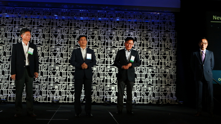
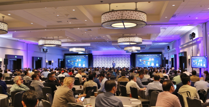
Kinam Kim, President of Samsung Electronics’ Semiconductor Business, detailed the company’s foundry process foundry roadmap at the Samsung Foundry Forum 2017. The 8nm LPP (Low Power Plus) process is claimed to offer the most competitive solution before transitioning to EUV (Extreme Ultra Violet) process, offering improved gate density and performance compared to the 10nm LPP process.
The 7nm LPP fabrication process from Samsung will be the first to offer EUV lithography solution, and it has been developed in collaboration with Dutch photolithography systems company ASML. The South Korean semiconductor giant claimed that its 7nm LPP process would “break the barriers of Moore’s Law scaling.” The company’s 6nm LPP, 5nm LPP, and 4nm LPP processes will offer even better power efficiency.
While the 6nm LPP process will be an improvement to the 7nm EUV process, adopting Samsung’s unique Smart Scaling solutions, the 5nm LPP process will extend the physical scaling limit of the FinFET process. The 4nm LPP process will be the first implementation of Samsung’s next-generation architecture – MBCFET structure (Multi-Bridge Channel FET) – that uses a Nanosheet device to overcome physical scaling limitation of the FinFET process.
The company also talked about its plans for the 18nm FD-SOI (Fully Depleted – Silicon on Insulator) process technology, which is claimed to be well-suited for IoT devices. The company will expand the 28nm FDS technology by incorporating RF (Radio Frequency) and eMRAM(embedded Magnetic Random Access Memory) options. The 18nm FD-SOI process will be an improvement over the 28nm FDS process with improved power efficiency, area, and performance.
Jong Shik Yoon, Executive Vice President of the Foundry Business at Samsung Electronics, said, “The ubiquitous nature of smart, connected machines and everyday consumer devices signals the beginning of the next industrial revolution. To successfully compete in today’s fast-paced business environment, our customers need a foundry partner with a comprehensive roadmap at the advanced process nodes to achieve their business goals and objectives.”